What is PCB Assembly Process: A Clear Explanation
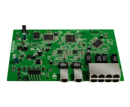
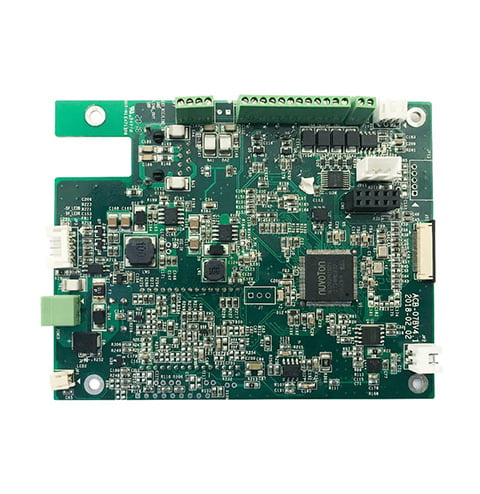
If you’re interested in electronics manufacturing, you might have heard of PCB assembly process. PCB stands for Printed Circuit Board, which is a key component in most electronic devices. The PCB assembly process involves transforming the raw PCB into a populated board that can perform designated functions. This process is essential in electronics manufacturing as it turns a PCB into the brain or backbone of an electronic device.

The PCB assembly process is a complex series of steps that involves multiple stages. The process starts with the design and manufacturing of the PCB, followed by material preparation, SMT and THT processes, and post-assembly services. Each stage of the process requires careful attention to detail, as even minor errors can lead to significant problems down the line. The goal of the PCB assembly process is to create a functional device according to the design specifications.
Overview of PCB Assembly

Definition and Purpose
PCB assembly (PCBA) is the process of assembling electronic components onto a printed circuit board (PCB) to form a complete functional device. The purpose of PCBA is to transform the bare PCB, which is little more than a piece of fiberglass, into a functional device that can perform designated functions. PCBA is an essential step in electronics manufacturing, as it turns the PCB into the brain or backbone of an electronic device.
The PCBA process involves several stages, including component placement, soldering, inspection, and testing. The process is defined according to the device standards, so it can be automated or manual. The PCBA process is critical to the success of an electronic device, as it ensures that the device is reliable, efficient, and performs as intended.
Key Components
PCBA involves the assembly of various electronic components onto a PCB. The key components include:
- Printed Circuit Board (PCB): The PCB is the foundation of the electronic device. It provides a platform for mounting electronic components and serves as a pathway for electrical signals to flow between the components.
- Electronic Components: These are the various components that are mounted onto the PCB. They include resistors, capacitors, diodes, transistors, integrated circuits, and other specialized components.
- Solder: Solder is used to join the electronic components to the PCB. It is a metal alloy that melts at a low temperature and solidifies to form a permanent bond between the component and the PCB.
- Flux: Flux is a chemical agent that is used to clean and prepare the surfaces of the PCB and the electronic components before soldering. It helps to remove any oxidation or contamination that may interfere with the soldering process.
- Solder Paste: Solder paste is a mixture of solder and flux that is used to apply solder to the PCB. It is applied to the PCB using a stencil, and the electronic components are then placed onto the solder paste.
PCB assembly is a complex process that requires specialized equipment, skilled technicians, and strict quality control measures. The success of the PCBA process depends on the quality of the components, the accuracy of the assembly process, and the thoroughness of the testing and inspection procedures.
Preparation for Assembly

Before the PCB assembly process can begin, there are several steps that must be taken to ensure that the process runs smoothly. These include material procurement, PCB design and layout, and solder paste application.
Material Procurement
The first step in preparing for the PCB assembly process is to procure all the necessary materials. This includes the PCB itself, as well as all the components that will be used to populate the board. It is important to ensure that all the components are of the correct type and that they are compatible with the PCB.
To make sure that you have all the components that you need, you should create a Bill of Materials (BOM). The BOM should list all the components that are required for the assembly process, along with their part numbers and quantities. Once you have the BOM, you can begin the process of procuring the components.
PCB Design and Layout
The next step in preparing for the PCB assembly process is to design and layout the PCB. This involves creating a schematic diagram of the circuit and then using this to create a physical layout of the board.
When designing the PCB, it is important to take into account factors such as the size and shape of the board, the number and type of components that will be used, and the electrical requirements of the circuit. Once the design is complete, it can be used to create the physical layout of the board.
Solder Paste Application
The final step in preparing for the PCB assembly process is to apply solder paste to the board. This is done using a stencil that is placed over the board and then used to apply the paste to the appropriate areas.
When applying the solder paste, it is important to ensure that the correct amount is used and that it is applied evenly across the board. This will help to ensure that the components are properly secured to the board during the assembly process.
In summary, preparing for the PCB assembly process involves procuring all the necessary materials, designing and laying out the PCB, and applying solder paste to the board. By taking the time to properly prepare for the assembly process, you can help to ensure that it runs smoothly and that the final product is of the highest quality.
Assembly Process
The PCB assembly process is a crucial step in the manufacturing of electronic devices. It involves populating the circuit board with all the necessary components, including resistors, capacitors, and integrated circuits. Here are the main steps involved in the assembly process:
Pick and Place
The pick and place process involves the use of automated machines to place the components onto the circuit board accurately. The machine uses a nozzle to pick up the components from a reel or tray and place them onto the board. The machine can place components of different sizes, shapes, and packages. The machine can place thousands of components per hour, making it an efficient process.
Soldering
Soldering is the process of attaching the components to the circuit board using solder. The solder is a metal alloy that melts when heated, creating a bond between the component and the board. There are two types of soldering methods: through-hole and surface mount. Through-hole soldering involves inserting the component leads through holes in the board and soldering them on the other side. Surface mount soldering involves placing the component on the surface of the board and soldering it in place.
Inspection and Quality Control
Inspection and quality control are essential steps in the assembly process. The board undergoes visual inspection to ensure that all the components are in the right place, and there are no soldering defects. Automated optical inspection (AOI) machines are used to detect any issues with the board. The board is also tested to ensure that it functions correctly.
In conclusion, the PCB assembly process involves several steps, including pick and place, soldering, and inspection. The process requires precision, accuracy, and attention to detail to ensure that the final product is of high quality.
Testing and Functionality Verification
Once the PCB has been assembled, it is important to verify that it works as intended. There are two main types of testing that are commonly used in PCB assembly: in-circuit testing and functional testing.
In-Circuit Testing
In-circuit testing is a type of testing that is performed while the PCB is still in the assembly process. This type of testing is used to verify that each component on the PCB is correctly placed and soldered. In-circuit testing is typically performed using a bed-of-nails tester, which is a specialized piece of equipment that uses a series of probes to make contact with specific points on the PCB.
During in-circuit testing, the bed-of-nails tester sends electrical signals through the PCB and measures the response. This allows the tester to identify any components that are not properly connected or that are not functioning as intended. In-circuit testing is an important step in the PCB assembly process, as it can help to identify issues early on and prevent costly rework later on.
Functional Testing
Functional testing is a type of testing that is performed after the PCB has been fully assembled. This type of testing is used to verify that the PCB functions as intended, with all components and circuits operating correctly. Functional testing is typically performed using specialized test equipment, such as a functional tester or a flying probe tester.
During functional testing, the tester sends a series of signals through the PCB and measures the response. This allows the tester to identify any issues with the PCB’s functionality, such as components that are not functioning as intended or circuits that are not properly connected. Functional testing is a critical step in the PCB assembly process, as it ensures that the PCB will work as intended once it is deployed in the field.
In summary, testing and functionality verification are critical steps in the PCB assembly process. In-circuit testing is used to verify that each component on the PCB is correctly placed and soldered, while functional testing is used to verify that the PCB functions as intended. By performing these tests, manufacturers can ensure that their PCBs are of high quality and will work as intended in the field.
Final Assembly and Packaging
After the PCB components are soldered onto the board, the next step in the PCB assembly process is the final assembly and packaging. This step involves enclosing the board in a protective casing, performing a final inspection, and packaging the board for shipping.
Board Enclosure
The first step in final assembly is to enclose the board in a protective casing. This casing can be made of various materials, such as plastic, metal, or even wood. The casing protects the board from physical damage and environmental factors such as dust, moisture, and temperature changes.
Final Inspection
Once the board is enclosed in its casing, it undergoes a final inspection to ensure that it meets the required standards. This inspection involves checking for any defects or faults in the board, such as missing components, incorrect placement, or soldering defects. The board is also tested to ensure that it functions properly.
Packaging and Shipping
After the board has passed the final inspection, it is ready to be packaged and shipped to the customer. The packaging process involves placing the board in a protective container, such as a box or envelope, and adding any necessary documentation, such as an instruction manual or warranty information. The package is then labeled with the customer’s address and shipped to its destination.
Overall, the final assembly and packaging step is a crucial part of the PCB assembly process. It ensures that the board is protected, functional, and ready for use by the customer.


