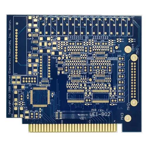
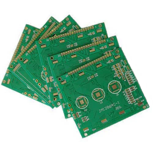
Double-sided gold finger circuit board
Name: Double-sided gold finger circuit board
Plate: FR4
Layers: 2L
Material: S1141
Plate thickness: 1.6mm
Copper thickness of inner and outer layers: 1oz
Minimum aperture: 0.3mm
Surface Treatment: Immersion Gold
Line width: 0.15mm
Line distance: 0.15mm
Others: electroplating gold fingers
Blind hole structure: L1-L2
Use: board, interface
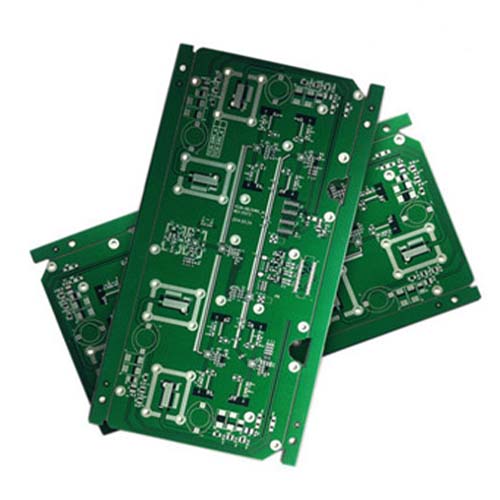
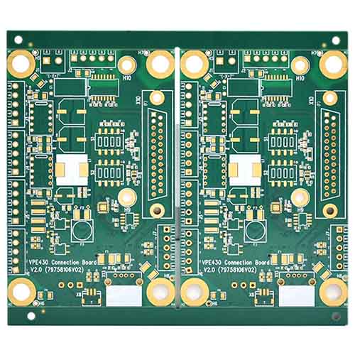
Double-sided industrial control PCB board
Name: Double-sided industrial control PCB board
Sheet: FR-4
Plate thickness: 1.0mm
Layers: 2L
Size: 79.48*35.6mm
Minimum aperture: 0.332mm
Line width/moment: 0.42*0.46mm
Copper foil thickness: 1/1OZ
Surface treatment: lead-free spray tin
Solder mask/character: green oil white character
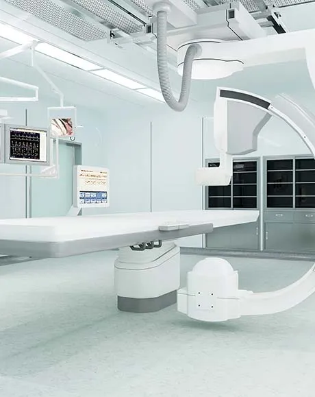
Name: Medical Device PCB Board
Plate: Shengyi S1000H
Plate thickness: 1.6mm
Number of layers: four-layer board
Size: 216.3*92.6mm
Minimum aperture: 0.1mm
Line width/moment: 0.1/0.1mm
Copper foil thickness: 1/1/1/1oz
Surface treatment: Immersion silver
Solder mask/character: green oil white character
LCD liquid crystal display PCB circuit board
Name: LCD liquid crystal display PCB circuit board
Plate: KB6165F
Plate thickness: 1.6mm
Layers: 2L
Copper Foil: 1.0 oz
Process: Immersion Gold 2U
Size: 147.2*65mm
Minimum aperture: 0.22mm
Line width/moment: 0.3*0.27mm
Copper foil thickness: 1/1OZ
Surface treatment: lead-free spray tin
Solder mask/character: green oil white character
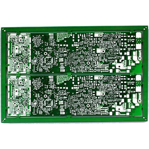
Name: TG150 PCB circuit board
Material: TG150
Layers: four layers
Drilling diameter: 0.2mm
Minimum line width: 0.08mm
Minimum line spacing: 0.1mm
Process: Immersion Gold
Features: Compared with TG130, the heat resistance, moisture resistance, chemical resistance, stability and other characteristics of PCB printed boards will be improved
Wireless doorbell PCB circuit board
Name: Wireless doorbell PCB circuit board
Plate: KB6165F
Plate thickness: 1.0mm
Layers: 2L
Size: 79.48*35.6mm
Minimum aperture: 0.332mm
Line width/moment: 0.42*0.46mm
Copper foil thickness: 1/1OZ
Surface treatment: lead-free spray tin
Solder mask/character: green oil white character
- PCB Manufacturing Capability
- PCB manufacturing equipment
| Standard PCB Production Capability | |
| Feature | Capability |
| Quality Grade | Standard IPC 2 |
| Number of Layers | 1 – 32layers |
| Order Quantity | 1pcs – 10,000,000 pcs |
| Build Time | 2days – 5weeks (Expedited Service) |
| Material | FR-4 Standard Tg 150°C, FR4-High Tg 170°C, FR4-High-Tg 180°C, FR4-Halogen-free, FR4-Halogen-free & High-Tg |
| Board Size | Min 6*6mm | Max 600*700mm |
| Board size tolerance | ±0.1mm – ±0.3mm |
| Board Thickness | 0.4mm – 3.2mm |
| Board Thickness Tolerance | ±0.1mm – ±10% |
| Copper Weight | 0.5oz – 6.0oz |
| Inner Layer Copper Weight | 0.5oz – 2.0oz |
| Copper Thickness Tolerance | +0μm +20μm |
| Min Tracing/Spacing | 3mil/3mil |
| Solder Mask Sides | As per the file |
| Solder Mask Color | Green, White, Blue, Black, Red, Yellow |
| Silkscreen Sides | As per the file |
| Silkscreen Color | White, Blue, Black, Red, Yellow |
| Surface Finish | HASL – Hot Air Solder Leveling |
| Lead Free HASL – RoHS | |
| ENIG – Electroless Nickle/Immersion Gold – RoHS | |
| ENEPIG – Electroless Nickel Electroless Palladium Immersion Gold – RoHS | |
| Immersion Silver – RoHS | |
| Immersion Tin – RoHS | |
| OSP -Organic Solderability Preservatives – RoHS | |
| Min Annular Ring | 3mil |
| Min Drilling Hole Diameter | 6mil, 4mil-laser drill |
| Min Width of Cutout (NPTH) | 0.8mm |
| NPTH Hole Size Tolerance | ±.002″ (±0.05mm) |
| Min Width of Slot Hole (PTH) | 0.6mm |
| PTH Hole Size Tolerance | ±.003″ (±0.08mm) – ±4mil |
| Surface/Hole Plating Thickness | 20μm – 30μm |
| SM Tolerance (LPI) | .003″ (0.075mm) |
| Aspect Ratio | 1.10 (hole size: board thickness) |
| Test | 10V – 250V, flying probe or testing fixture |
| Impedance tolerance | ±5% – ±10% |
| SMD Pitch | 0.2mm(8mil) |
| BGA Pitch | 0.2mm(8mil) |
| Chamfer of Gold Fingers | 20, 30, 45, 60 |
| Other Techniques | Gold fingers |
| Blind and Buried Holes | |
| peelable solder mask | |
| Edge plating | |
| Carbon Mask | |
| Kapton tape | |
| Countersink/counterbore hole | |
| Half-cut/Castellated hole | |
| Press fit hole | |
| Via tented/covered with resin | |
| Via plugged/filled with resin | |
| Via in pad | |
| Electrical Test | |

PCB Drilling machine

PCB pattern plating line

PCB solder mask expose machine

PCB pattern expose machine

Strip film etching line

Solder mask screen silk print machine

Solder mask scrubbing line

PCB Flying Probe Test (FPT)

Fully automatic exposure machine

we provide 24-hour service and support, you will receive a reply to your question within 2 hours and a quotation within 24 hours.

Own PCB factory of 50,000 square meters, the monthly output can reach 60,000 square meters, no minimum PCB order requirements

Before the official production of the PCB, we will conduct a free DFM review service and support free Allegro, Altium, Protel, PADS, OBD, Gerber and other formats.

We can provide you with high frequency, high TG, high CTI, buried blind via, aluminum based PCB manufacturing, the quality is fully compliant with IPC 610-D standard, testing and quality assurance
We support Double-sided gold finger circuit board business, LEIYAO is a professional one-stop PCBA ...
Industrial control product PCB: PCB circuit board that controls the normal operation of equipment in...
LEIYAO supports Medical Device PCB Board business, we are a professional PCBA one-stop assembly fa...
We provide LCD liquid crystal display PCB circuit board services. LEIYAO is your one stop turnkey ...
We support TG150 PCB circuit board business, LEIYAO is a professional one-stop PCBA service factor...
LEIYAO provides Wireless doorbell PCB circuit board services. This is a PCBA one-stop assembly fac...