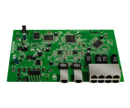
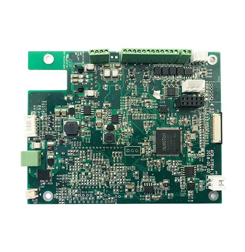
What is meant by PCB Design and SMT Electronic Components?
Modern electronics production is dependent on PCB design and SMT electrical components. Let’s explore each subject in more detail:
-
PCB design and SMT electrical components:
A printed circuit board (PCB) design lays out and connects electronic components on a board. It is a base for mounting and connecting electrical parts to build working circuits. The following are some essential PCB design points:
-
Software Tools:
Specialized software programs like Altium Designer, Cadence Allegro, Eagle, KiCad, etc., are frequently used in PCB design. These tools include a variety of functions for planning the circuit layout, producing production files, establishing component footprints, and routing traces.
-
Circuit Schematic:
Developing a circuit schematic using schematic capture software is typical before designing a PCB. The schematic acts as a guide throughout the PCB designing process and depicts the logical links between components.
-
Component Positioning:
When placing electronic components on a PCB, PCB designers consider various issues, including component size, electrical connections, signal integrity, thermal management, and manufacturability.
-
Routing:
After placing the components, the designer arranges the traces (copper tracks) such that the components are electrically connected. Optimizing trace lengths, staying clear of signal interference, and ensuring enough space between traces to prevent short circuits are all steps in the routing process. PCB design must abide by design regulations and limitations of the manufacturing process, such as minimum trace width, clearance requirements, via standards, and layer stack-up parameters.
-
Design Verification:
Designers design rule checks (DRC) and simulate the circuit to confirm its functionality, signal integrity, and thermal concerns before manufacturing the PCB design.
-
Manufacturing Files:
After the design is complete, the PCB design software creates manufacturing files, such as bill of materials (BOM) sheets that list the parts needed for assembly, drill files that describe the positions of holes, and Gerber files that provide copper information particular to each layer.
SMT Electronic Components:
-
Package forms:
PCB Design and SMT Electronic Components are available in a variety of package forms, including chip scale package (CSP), ball grid array (BGA), tiny outline integrated circuit (SOIC), and quad flat no leads (QFN). Specific dimensions, pin arrangements, and soldering requirements apply to each package type.
-
Component Size:
Since SMT components are often smaller than through-hole components, electronic devices can be made smaller with a higher component density on the PCB.
-
Soldering Methods for PCB design and SMT electrical components:
Reflow soldering is a method for attaching SMT components to PCBs in which solder paste is put to the board, and the components are heated to melt the solder and create electrical connections. Alternatively, components that cannot tolerate the high temperatures of reflow soldering are soldered using selective soldering or wave soldering methods.
-
Component Handling:
Handling SMT components properly requires antistatic measures, automated pick-and-place equipment, and cautious storage to prevent damage because of their small size and fragile nature.
-
SMT Manufacturing Equipment:
To achieve precise component placement and high-quality solder joints, SMT assembly requires specialized equipment such as pick-and-place machines, solder paste dispensers, reflow ovens, and inspection systems.
Why are PCB Design and SMT Electronic Components Essential for Electronic Devices?
- Helps in mounting and connecting electrical components.
- Gives a small, well-organized structure for effective circuits.
- Allows for the arrangement of components to be optimized for performance.
- Assures appropriate signal flow and electrical connections.
- Enables upgrades and alterations to the design as it is being developed.
- Higher component density and miniaturization are made possible by smaller sizes.
- Shorter electrical channels that provide high-speed performance.
- Enhanced signal integrity is achieved by reducing parasitic capacitance and inductance.
- Automates assembly processes to increase cost-effectiveness.
- Enables effective thermal management and heat dispersion.
- Increases resistance to vibration and mechanical stability.
- Allows for dependable and long-lasting soldered connections.


