PCB Assembly Full Form: What Does PCB Stand For in Electronics Manufacturing?
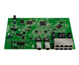
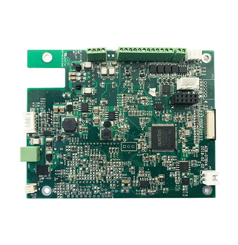
If you’re working in the electronics industry, you’ve likely heard the term “PCB assembly” before. PCB stands for “printed circuit board,” and PCB assembly is the process of mounting electronic components to a PCB. This process is crucial for creating functional electronic devices, as the PCB acts as the “brain” of the device, connecting all of the components together.

The PCB assembly process involves several steps, including component placement, soldering, and inspection. During component placement, the electronic components are arranged on the PCB according to a specific design. Soldering is then used to attach the components to the PCB, creating a permanent connection. Finally, the PCB is inspected to ensure that all of the components are properly mounted and that there are no defects or issues that could cause the device to malfunction.
Basics of PCB Assembly

Definition of PCB Assembly
PCB Assembly (PCBA) is the process of assembling electronic components onto a printed circuit board (PCB) to create a fully functional electronic device. The process of PCB assembly includes several steps, such as component placement, soldering, inspection, and testing. These steps are performed to ensure that the final product meets the design specifications and is free from defects.
Components of PCB Assembly
PCB Assembly consists of several components that are essential for creating a functional electronic device. These components include:
- Printed Circuit Board (PCB): A PCB is the foundation of any electronic device. It is a flat board made of fiberglass or plastic that contains copper tracks and pads. These tracks and pads are used to connect electronic components and circuits together.
- Electronic Components: Electronic components are the building blocks of any electronic device. These components include resistors, capacitors, diodes, transistors, and integrated circuits (ICs).
- Soldering Materials: Soldering is the process of joining two metal surfaces using a filler material called solder. Soldering materials include solder paste, solder wire, and flux.
- Testing Equipment: Testing equipment is used to test the functionality of the electronic device. This equipment includes oscilloscopes, multimeters, and function generators.
PCB Assembly is a complex process that requires a high level of skill and expertise. The process involves several steps, and each step must be performed with precision to ensure that the final product meets the design specifications.
PCB Assembly Process

When it comes to PCB assembly, there are several key steps that must be followed to ensure a successful outcome. These steps include solder paste stenciling, pick and place, reflow soldering, manual assembly and inspection, and testing and quality control.
Solder Paste Stenciling
The first step in the PCB assembly process is solder paste stenciling. This involves applying solder paste to the PCB using a stencil. The stencil is placed over the PCB and the paste is pushed through the stencil and onto the board. This step is critical because it ensures that the solder paste is applied evenly and accurately.
Pick and Place
The next step in the process is pick and place. This involves placing the components onto the PCB. This can be done manually or with the help of a pick and place machine. This step is important because it ensures that the components are placed in the correct location and orientation.
Reflow Soldering
Once the components are in place, the next step is reflow soldering. This involves heating the PCB and components to a specific temperature to melt the solder paste and create a permanent bond between the components and the PCB. This step is critical because it ensures that the components are securely attached to the PCB.
Manual Assembly and Inspection
In some cases, manual assembly and inspection may be required. This involves manually soldering components onto the PCB and inspecting the board to ensure that everything is in place and functioning properly. This step is important because it ensures that any issues or defects are caught and corrected before the board is completed.
Testing and Quality Control
The final step in the PCB assembly process is testing and quality control. This involves testing the board to ensure that it functions properly and meets all specifications. This step is critical because it ensures that the board is of high quality and will perform as expected.
The PCB assembly process is a complex and multi-step process that requires careful attention to detail and precision. By following the steps outlined above, you can ensure that your PCB is assembled correctly and functions properly.
Types of PCB Assembly
When it comes to PCB assembly, there are three main types to consider. Each type has its own unique benefits and drawbacks, and the best choice for your project will depend on a variety of factors, including the complexity of the design, the intended use of the device, and the available budget.
Through-Hole Technology
Through-hole technology (THT) is the oldest and most traditional method of PCB assembly. As the name suggests, this type of assembly involves inserting components through holes in the circuit board and then soldering them in place. This method is known for its durability and reliability, as the components are securely anchored to the board. However, THT can be time-consuming and expensive, as it requires manual labor to insert and solder the components.
Surface-Mount Technology
Surface-mount technology (SMT) is a newer and more popular method of PCB assembly. With SMT, components are mounted directly onto the surface of the board, rather than being inserted through holes. This method is faster and more cost-effective than THT, as it can be automated and requires less manual labor. SMT also allows for smaller and more compact designs, as the components take up less space on the board. However, SMT can be less durable than THT, as the components are not as securely anchored to the board.
Mixed Technology PCB Assembly
As the name suggests, mixed technology PCB assembly involves a combination of both THT and SMT methods. This approach allows for the benefits of both methods, while minimizing their drawbacks. For example, THT can be used for components that require extra durability and reliability, while SMT can be used for smaller and more compact components. Mixed technology PCB assembly can be more complex and time-consuming than either THT or SMT alone, but it can also provide the best of both worlds.
In summary, the type of PCB assembly you choose will depend on a variety of factors, including the complexity of the design, the intended use of the device, and the available budget. THT is known for its durability and reliability, while SMT is faster and more cost-effective. Mixed technology PCB assembly can provide the benefits of both methods, but can also be more complex and time-consuming.
PCB Assembly Equipment
When it comes to PCB assembly, there are two main types of equipment used: automated assembly machinery and inspection and testing equipment.
Automated Assembly Machinery
Automated assembly machinery is used to place and solder components onto the PCB. This machinery includes pick-and-place machines, which use suction cups to pick up components and place them onto the PCB, and reflow ovens, which use heat to melt the solder and attach the components to the board.
Modern pick-and-place machines are highly accurate and can place components at a rate of thousands per hour. They can handle a wide range of component sizes and shapes, from tiny surface-mount resistors to large ICs with dozens of pins.
Reflow ovens come in several different types, including convection ovens, vapor-phase ovens, and infrared ovens. Each type has its own advantages and disadvantages, but all are designed to heat the PCB and components to a precise temperature and then cool them down gradually to prevent thermal shock.
Inspection and Testing Equipment
After the components have been placed and soldered, the PCB must be inspected and tested to ensure that it is functioning correctly. This is done using a variety of inspection and testing equipment, including:
- Automated optical inspection (AOI) machines, which use cameras and software to detect defects such as missing components, incorrect component orientation, and solder bridges.
- X-ray machines, which can inspect the inside of components and the solder joints to detect defects such as voids and cracks.
- Flying probe testers, which use probes to test the electrical connections between components on the PCB.
- In-circuit testers, which test the electrical characteristics of individual components on the PCB.
- Functional testers, which test the overall functionality of the PCB by simulating the conditions under which it will be used.
By using these advanced inspection and testing equipment, PCB manufacturers can ensure that their products meet the highest standards of quality and reliability.
Challenges in PCB Assembly
PCB assembly is a complex process that involves multiple stages of manufacturing, testing, and quality control. The process requires precision, accuracy, and attention to detail to ensure that the final product meets the required specifications. However, there are several challenges that can arise during the PCB assembly process that can impact the functionality, reliability, and quality of the final product. In this section, we will discuss some of the most common challenges in PCB assembly and how to overcome them.
Complexity and Miniaturization
One of the biggest challenges in PCB assembly is the increasing complexity and miniaturization of electronic devices. As electronic devices become smaller and more complex, the components used in PCB assembly become more miniature and densely packed. This makes it more difficult to place and solder components onto the PCB, and increases the risk of errors and defects. To overcome this challenge, manufacturers need to use advanced equipment and techniques, such as automated pick-and-place machines, X-ray inspection, and 3D printing.
Heat Management
Another challenge in PCB assembly is heat management. As electronic devices become more powerful, they generate more heat, which can damage the components and reduce the overall lifespan of the device. To overcome this challenge, manufacturers need to use heat-resistant materials and techniques, such as thermal vias, heat sinks, and thermal pads. They also need to ensure that the PCB design allows for proper airflow and heat dissipation.
Quality Assurance
Finally, quality assurance is a critical challenge in PCB assembly. As electronic devices become more complex and miniaturized, the risk of defects and errors increases. Manufacturers need to implement rigorous quality control measures throughout the entire PCB assembly process, including visual inspection, automated testing, and functional testing. They also need to use high-quality materials and components, and ensure that their suppliers meet strict quality standards.
In summary, PCB assembly is a complex process that requires precision, accuracy, and attention to detail. Manufacturers need to overcome several challenges, including complexity and miniaturization, heat management, and quality assurance, to produce high-quality electronic devices that meet the required specifications.


