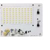
LED Lightening High Volume PCB Assembly Leadsintec
Name: LED Lightening High Volume PCB Assembly Leadsintec
Origin: China
Certified: UL, CE, RoHS
Base Material: FR-4/aluminum/ceramic/cem-3/FR-1
Solder mask: White Black Green Blue Red
Application: LED Lighting
Surface Finishing: HASL\OSP\immersion Gold
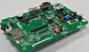
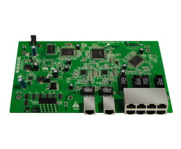
Gaming Console High Volume PCB Assembly
Name: Gaming Console High Volume PCB Assembly
Origin: China
Certified: UL, CE, RoHS
Layers: 1L
Base Material: FR-4
Board Thickness: customized
Copper Thickness: 1oz
Surface Finishing: Lead Free HASL
Application: for gaming
Computer Motherboard High Volume PCB Assembly- Leadsintec
Name: Computer Motherboard High Volume PCB Assembly- Leadsintec
Origin: China
Certified: UL, CE, RoHS
Copper Thickness: 1/3OZ – 4OZ o
Material: FR4
Surface Finishing: HASL\OSP\immersion Gold
applications: for computer devices
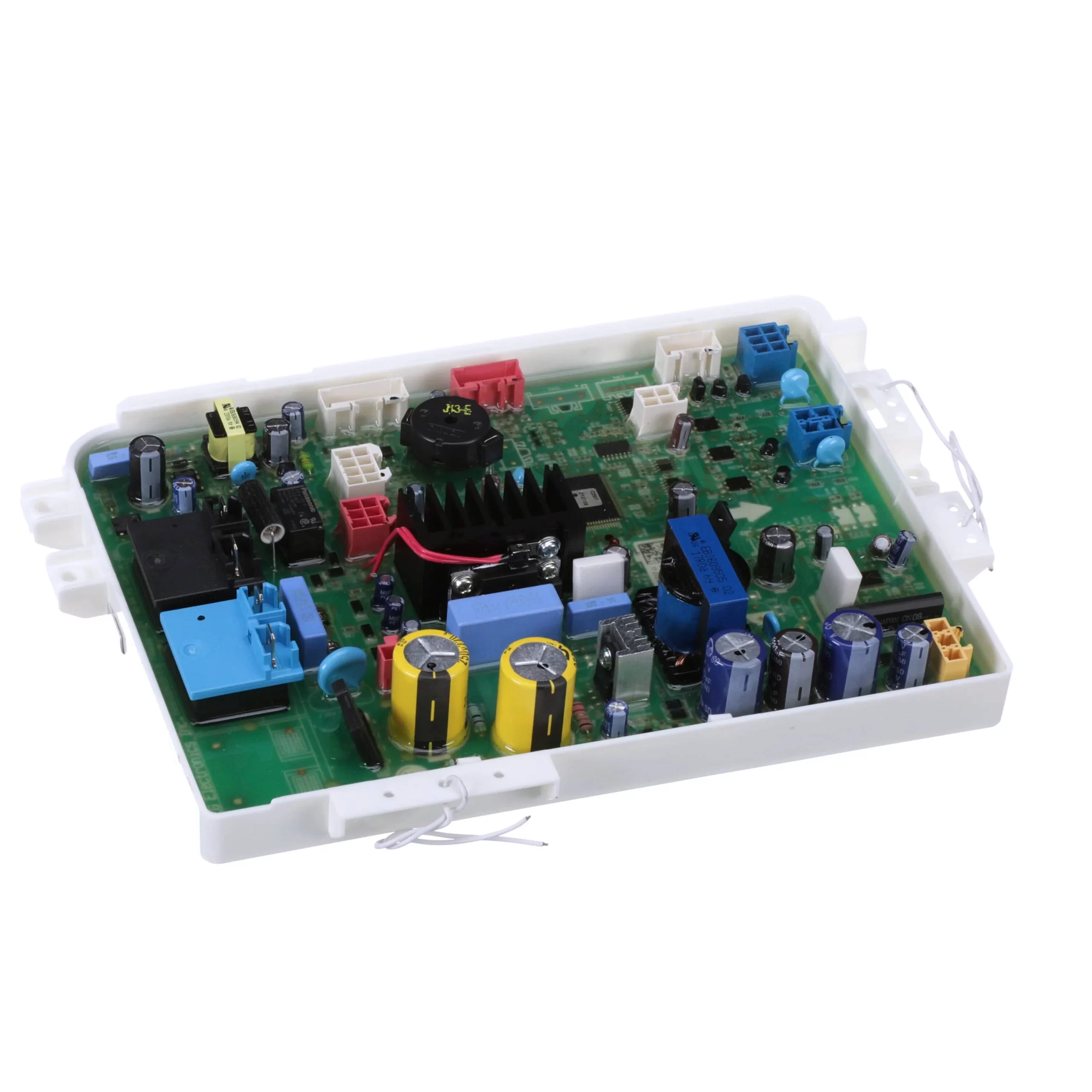
Dishwasher main control High Volume PCB Assembly – One Stop Service
Name: Dishwasher main control High Volume PCB Assembly – One Stop Service
Origin: China
Certified: UL, CE, RoHS
Board thickness: customized
Surface finish: HASL/ lead-free HASL
Solder mask :green, blue, white, red, etc
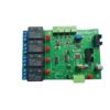
TV Motherboard High Volume PCB Assembly
Name: TV Motherboard High Volume PCB Assembly
Origin: China
Certified: UL, CE, RoHS
Surface Finishing: HASL\OSP\immersion Gold
Copper Thickness: 1-5 OZ
applications: electronic product
Board thickness: customized
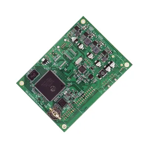
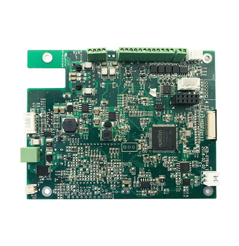
Smartphones Motherboard High volume PCB
Name: Smartphones Motherboard High volume PCB
Origin: China
Certified: UL, CE, RoHS
Solder resist color: Green; Red; Yellow; Black; White
Material: FR4 CEM1 CEM3 Hight TG
Application: Electronic product
Board thickness: customized
- PCB Assembly Capability
- PCB Assembly Equipment
High Volume PCB Assembly is a specialized electronic manufacturing service designed to meet the demands of large-scale production. It involves the efficient and rapid assembly of printed circuit boards (PCBs) in high quantities to meet the requirements of industries. It includes consumer electronics, automotive, also telecommunications, and more.
High Volume PCB utilizes advanced automated assembly processes, state-of-the-art equipment, and streamlined production workflows to ensure the fast and accurate assembly of PCBs. It also involves the mounting of various electronic components onto the PCB. This includes integrated circuits (ICs), resistors, capacitors, connectors, and more.
Advantages of High-Volume PCB Assembly:
- Efficient Production: High Volume Assembly is specifically designed for efficient production in large quantities. The utilization of automated pick-and-place machines, soldering equipment, and inspection systems allows for rapid assembly. It also reduces manufacturing lead times and increases production throughput.
- Consistency and Quality Control: High Volume Assembly employs robust quality control measures to ensure consistency and reliability in the assembled PCBs. Automated inspection systems perform checks for component placement accuracy, solder joint quality, and other critical parameters. This also enables high-quality standards are met consistently across the production run.
- Cost-Effectiveness: With its optimized production processes and economies of scale, High Volume PCB Assembly offers cost-effective solutions for large-scale production. The automated assembly processes minimize labor costs, while efficient material management reduces waste and lowers overall production expenses.
- Scalability: High Volume PCB is highly scalable, making it suitable for both medium and large production runs. The streamlined processes and automated equipment allow for seamless scalability. This ensures that the production capacity can be adjusted to meet changing market demands.
- Design for Manufacturability (DFM): DFM principles are incorporated into the High Volume Assembly process to optimize the manufacturability of the PCB design. Design considerations such as component placement, PCB layout, and assembly constraints are evaluated to enhance the efficiency and quality of the assembly process.
| SMT capacity: 19 million points/day | ||
| Testing Equipment | X-RAY Nondestructive Tester, First Piece Tester, AOI Automatic Optical Tester, ICT Tester, BGA Rework Station | |
| Placement speed | Chip placement speed (at best conditions) 0.036 S/piece | |
| Mounted Component Specifications | Pasteable smallest package | |
| Minimum device accuracy | ||
| IC type chip accuracy | ||
| Mounted PCB Specifications | Substrate size | |
| Substrate thickness | ||
| throw rate | 1. Resistance-capacitance ratio 0.3% | |
| 2. IC type without throwing material | ||
| Board Type | POP/common board/FPC/rigid-flex board/metal substrate | |
| DIP daily production capacity | ||
| DIP plug-in production line | 50000 points/day | |
| DIP post welding production line | 20000 points/day | |
| DIP test production line | 50000pcs PCBA/day | |
| Assembly processing capability | ||
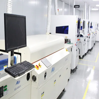
| The company has more than 10 advanced assembly production lines, dust-free and anti-static air-conditioning workshop, TP dust-free workshop, equipped with aging room, test room, functional test isolation room, advanced and perfect equipment, can carry out various product assembly, packaging, testing, Aging, etc. production. Monthly production capacity can reach 150,000 to 300,000 sets/month | ||
| PCBA processing capability | ||
| project | Mass processing capability | Small batch processing capability |
| Number of layers (max) | 2-18 | 20-30 |
| Plate type | FR-4, Ceramic Sheet, Aluminum Base Sheet PTFE, Halogen Free Sheet, High Tg Sheet | PTFE, PPO, PPE |
| Rogers,etc Teflon | E-65, ect | |
| Sheet mixing | 4 layers – 6 layers | 6th floor – 8th floor |
| biggest size | 610mm X 1100mm | / |
| Dimensional Accuracy | ±0.13mm | ±0.10mm |
| Plate thickness range | 0.2mm–6.00mm | 0.2mm–8.00mm |
| Thickness tolerance ( t≥0.8mm) | ±8% | ±5% |
| Thickness tolerance (t<0.8mm) | ±10% | ±8% |
| Media thickness | 0.076mm–6.00mm | 0.076mm–0.100mm |
| Minimum line width | 0.10mm | 0.075mm |
| Minimum spacing | 0.10mm | 0.075mm |
| Outer copper thickness | 8.75um–175um | 8.75um–280um |
| Inner layer copper thickness | 17.5um–175um | 0.15mm–0.25mm |
| Drilling hole diameter (mechanical drill) | 0.25mm–6.00mm | 0.15mm–0.25mm |
| Hole diameter (mechanical drill) | 0.20mm–6.00mm | 0.10mm–0.20mm |
| Hole Tolerance (Mechanical Drill) | 0.05mm | / |
| Hole tolerance (mechanical drill) | 0.075mm | 0.050mm |
| Laser Drilling Aperture | 0.10mm | 0.075mm |
| Plate thickness aperture ratio | 10:1 | 12:1 |
| Solder mask type | Photosensitive green, yellow, black, purple, blue, ink | / |
| Minimum Solder Mask Bridge Width | 0.10mm | 0.075mm |
| Minimum Solder Mask Isolation Ring | 0.05mm | 0.025mm |
| Plug hole diameter | 0.25mm–0.60mm | 0.60mm-0.80mm |
| Impedance tolerance | ±10% | ±5% |
| Surface treatment type | Hot air leveling, chemical nickel gold, immersion silver, electroplated nickel gold, chemical immersion tin, gold finger card board | Immersion Tin, OSP |
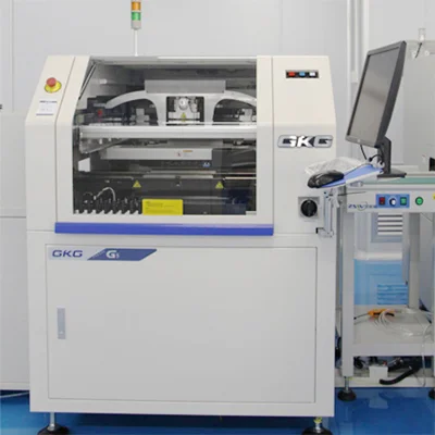
Automatic Solder Paste Printing Machine
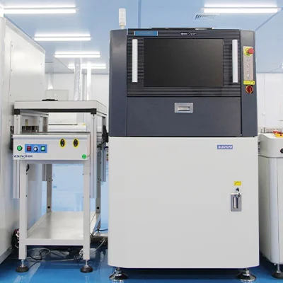
AOI Optical Inspection
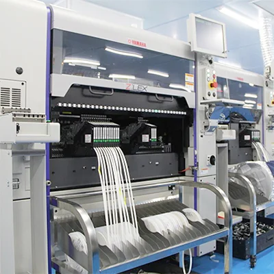
Smt High-Speed Placement Machine
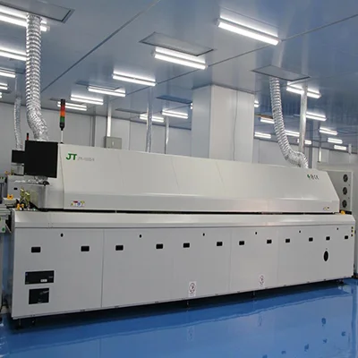
Nitrogen Reflow Soldering
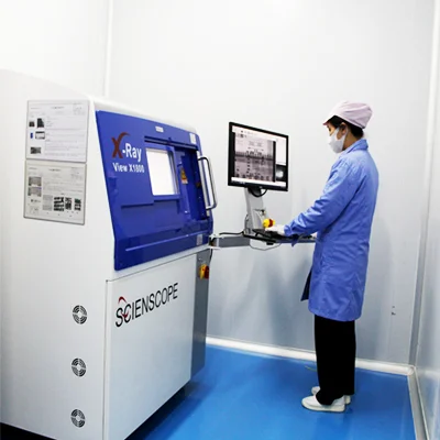
X-Ray
Three Anti-Paint Spraying Machine
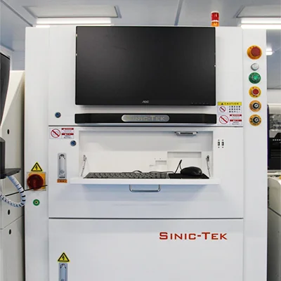
SPI Solder Paste Thickness Tester
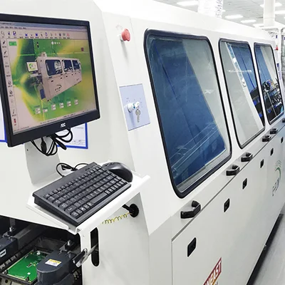
Automatic Wave Soldering Machine
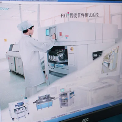
First Article Inspection

