- PCB manufacturing capability
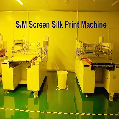
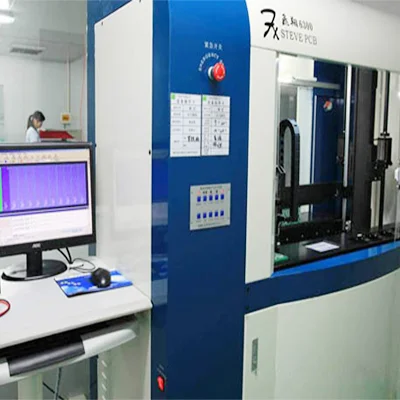
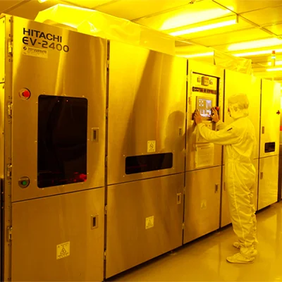
- PCB manufacturing equipment
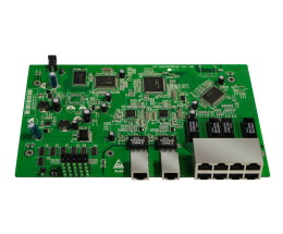
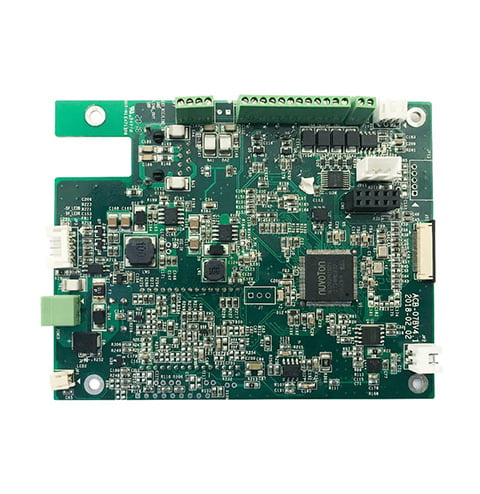
FR4 PCB (Printed Circuit Boards) are widely recognized as a reliable and versatile substrate for electronic applications. Constructed from a flame retardant grade 4 (FR4) epoxy laminate material, these PCBs offer excellent electrical performance and mechanical stability.
Our FR4 PCBs are engineered with precision and expertise to meet the highest industry standards. The FR4 material provides excellent electrical insulation and high dielectric strength, ensuring reliable performance and signal integrity.
With their mechanical stability, our FR4 PCB maintain their dimensional integrity even under demanding conditions, making them suitable for a wide range of environments.
Advantage of FR4 PCB:
- Cost-Effective Solution: FR4 PCBs offer a cost-effective solution for electronic projects. The availability of FR4 material and well-established manufacturing processes contribute to their affordability. This also makes them a practical choice for both prototyping and mass production.
- Wide Application Range: FR4 PCBs find applications in various industries, including consumer electronics, telecommunications, automotive, industrial equipment, and more. Their versatility allows them to support different electronic components and meet the requirements of diverse applications.
- Thermal Resistance: FR4 PCBs have good thermal resistance properties, enabling efficient heat dissipation. This also makes them suitable for applications that generate heat, helping to prevent component damage caused by overheating.
- Reliable Performance: FR4 PCBs are known for their reliability and durability. They can also withstand mechanical stress, vibrations, and impacts. This further ensures a long-lasting performance even in demanding environments.
- Excellent Electrical Performance: FR4 PCBs provide good electrical insulation and high dielectric strength, ensuring reliable performance and signal integrity. They also offer low loss tangent and high resistance to electrical breakdown. This moreover makes them suitable for high-frequency applications and complex circuit designs.
| Standard PCB Production Capability | |
| Feature | Capability |
| Quality Grade | Standard IPC 2 |
| Number of Layers | 1 – 32layers |
| Order Quantity | 1pcs – 10,000,000 pcs |
| Build Time | 2days – 5weeks (Expedited Service) |
| Material | FR-4 Standard Tg 150°C, FR4-High Tg 170°C, FR4-High-Tg 180°C, FR4-Halogen-free, FR4-Halogen-free & High-Tg |
| Board Size | Min 6*6mm | Max 600*700mm |
| Board size tolerance | ±0.1mm – ±0.3mm |
| Board Thickness | 0.4mm – 3.2mm |
| Board Thickness Tolerance | ±0.1mm – ±10% |
| Copper Weight | 0.5oz – 6.0oz |
| Inner Layer Copper Weight | 0.5oz – 2.0oz |
| Copper Thickness Tolerance | +0μm +20μm |
| Min Tracing/Spacing | 3mil/3mil |
| Solder Mask Sides | As per the file |
| Solder Mask Color | Green, White, Blue, Black, Red, Yellow |
| Silkscreen Sides | As per the file |
| Silkscreen Color | White, Blue, Black, Red, Yellow |
| Surface Finish | HASL – Hot Air Solder Leveling |
| Lead Free HASL – RoHS | |
| ENIG – Electroless Nickle/Immersion Gold – RoHS | |
| ENEPIG – Electroless Nickel Electroless Palladium Immersion Gold – RoHS | |
| Immersion Silver – RoHS | |
| Immersion Tin – RoHS | |
| OSP -Organic Solderability Preservatives – RoHS | |
| Min Annular Ring | 3mil |
| Min Drilling Hole Diameter | 6mil, 4mil-laser drill |
| Min Width of Cutout (NPTH) | 0.8mm |
| NPTH Hole Size Tolerance | ±.002″ (±0.05mm) |
| Min Width of Slot Hole (PTH) | 0.6mm |
| PTH Hole Size Tolerance | ±.003″ (±0.08mm) – ±4mil |
| Surface/Hole Plating Thickness | 20μm – 30μm |
| SM Tolerance (LPI) | .003″ (0.075mm) |
| Aspect Ratio | 1.10 (hole size: board thickness) |
| Test | 10V – 250V, flying probe or testing fixture |
| Impedance tolerance | ±5% – ±10% |
| SMD Pitch | 0.2mm(8mil) |
| BGA Pitch | 0.2mm(8mil) |
| Chamfer of Gold Fingers | 20, 30, 45, 60 |
| Other Techniques | Gold fingers |
| Blind and Buried Holes | |
| peelable solder mask | |
| Edge plating | |
| Carbon Mask | |
| Kapton tape | |
| Countersink/counterbore hole | |
| Half-cut/Castellated hole | |
| Press fit hole | |
| Via tented/covered with resin | |
| Via plugged/filled with resin | |
| Via in pad | |
| Electrical Test | |
PCB Drilling machine
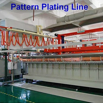
PCB pattern plating line
PCB solder mask expose machine
PCB pattern expose machine
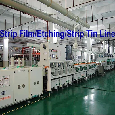
Strip film etching line
Solder mask screen silk print machine
Solder mask scrubbing line
PCB Flying Probe Test (FPT)
Fully automatic exposure machine

