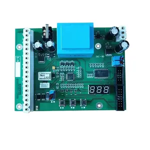
Hard Drives Double-sided PCB Assembly – PCBA Manufacturer
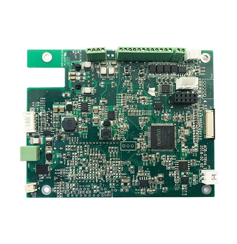
Name: Hard Drives Double-sided PCB Assembly – PCBA Manufacturer
Origin: China
Certified: UL, CE, RoHS
Copper Thickness: 0.5-50OZ
Base Material: FR4, High TG FR4, CEM-3, etc.
Layer: 2-50layers&above
Application: communication, automobile, industrial control, etc.

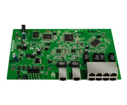
Printers Double-sided PCB Assembly – OEM Boards
Name: Printers Double-sided PCB Assembly – OEM Boards
Origin: China
Certified: UL, CE, RoHS
Material: FR4 Material
Layer: 1-64 Layers
Solder mask: Green. Black. Red. Yellow. White. Blue
Copper Thickness: 1 oz
Board Thickness: customized
Double sided PCB Especially Designed for traffic
Name: Double sided PCB Especially Designed for traffic
Origin: China
Certified: UL, CE, RoHS
Base Material: FR-4
Copper Thickness: 0.5oz–5oz, 0.5-5oz
Board Thickness: customized
applications: for traffic system
Surface Finishing: HASL
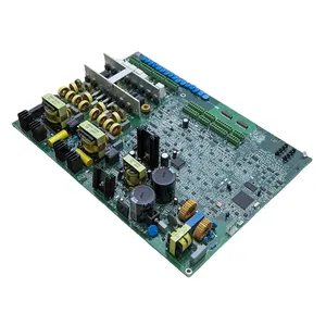
Phone System Double-sided PCB-Leadsintec
Name: Phone System Double-sided PCB-Leadsintec
Base Material: FR4
Copper Thickness: 1oz
Surface Finishing: HASL,ENIG,OSP
Number of Layers: 2
Application: Electronics Device
Solder mask color: Blue. green. red. black .white .etc
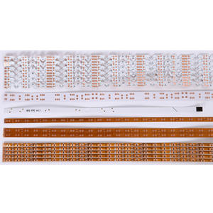
LED Lightening Double-sided PCB Assembly
Name: LED Lightening Double-sided PCB Assembly
Origin: China
Certified: UL, CE, RoHS
Surface Finishing: HASL LEAD FREE
Board Size: customized
Application: Christmas decorate lighting
Material: FR4 /aluminum/CEM1
Copper: 1-5 oz
Solder mask: White/Black/other customized
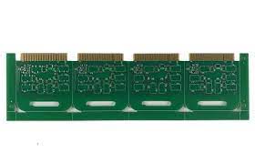
Reliable Double-sided PCB Manufacturer- Leadsintec
Name: Reliable Double-sided PCB Manufacturer- Leadsintec
Origin: China
Certified: UL, CE, RoHS
Layer: 1-22 Layers
Surface Finishing: HASL\OSP\immersion Gold
Base Material: FR4/ROGERS/Aluminum/High TG
Solder mask color: Green. Black. Red. Yellow. White. Blue. Purple. Matte Green.
- PCB Assembly Capability
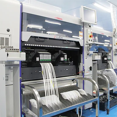
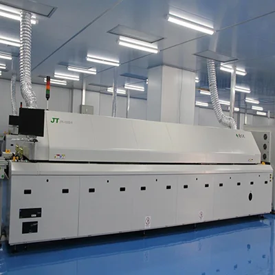
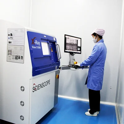
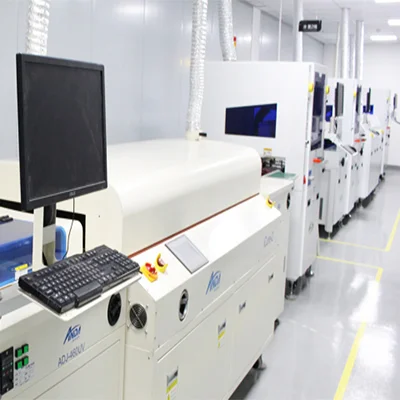
- PCB Assembly Equipment
Double-sided PCB assembly is a versatile and reliable electronic manufacturing process that involves the assembly of electronic components on both sides of a printed circuit board (PCB). With components mounted on both the top and bottom surfaces of the PCB, double-sided assembly allows for increased component density and enhanced functionality in electronic devices.
Double-sided PCB offers the capability to accommodate a larger number of electronic components, including integrated circuits (ICs), resistors, capacitors, connectors, and more. The components are mounted using various techniques such as surface mount technology (SMT), through-hole technology (THT), or a combination of both, depending on the design requirements and component specifications.
Advantages of Double-Sided PCB Assembly:
- Increased Component Density: Double-sided assembly allows for higher component density compared to single-sided assemblies. Utilizing both sides of the PCB provides more space for placing electronic components, enabling the design of more complex and feature-rich electronic devices.
- Enhanced Functionality: The additional space available in double-sided PCB assembly enables the inclusion of additional components, such as sensors, connectors, or specialized ICs, to enhance the functionality of the electronic device. This allows for the implementation of advanced features and improved performance.
- Improved Signal Integrity: Double-sided offers better signal integrity compared to single-sided PCBs. Routing signal traces on both sides of the PCB; helps reduce trace lengths and minimize electromagnetic interference (EMI), resulting in improved signal quality and reduced noise.
- Design Flexibility: Double-sided assembly provides design flexibility for complex electronic circuits. Designers have the freedom to route traces on both sides of the PCB, allowing for optimized signal flow, efficient power distribution, and effective separation of analog and digital components. This flexibility enables the creation of custom designs tailored to specific requirements.
- Ease of Repairs and Modifications: In the event of a faulty component or design change, double-sided PCB assembly offers convenience for repairs and modifications. Components mounted on either side of the PCB can be easily accessed and replaced, minimizing downtime and reducing the need for complete board replacement.
| SMT capacity: 19 million points/day | ||
| Testing Equipment | X-RAY Nondestructive Tester, First Piece Tester, AOI Automatic Optical Tester, ICT Tester, BGA Rework Station | |
| Placement speed | Chip placement speed (at best conditions) 0.036 S/piece | |
| Mounted Component Specifications | Pasteable smallest package | |
| Minimum device accuracy | ||
| IC type chip accuracy | ||
| Mounted PCB Specifications | Substrate size | |
| Substrate thickness | ||
| throw rate | 1. Resistance-capacitance ratio 0.3% | |
| 2. IC type without throwing material | ||
| Board Type | POP/common board/FPC/rigid-flex board/metal substrate | |
| DIP daily production capacity | ||
| DIP plug-in production line | 50000 points/day | |
| DIP post welding production line | 20000 points/day | |
| DIP test production line | 50000pcs PCBA/day | |
| Assembly processing capability | ||
| The company has more than 10 advanced assembly production lines, dust-free and anti-static air-conditioning workshop, TP dust-free workshop, equipped with aging room, test room, functional test isolation room, advanced and perfect equipment, can carry out various product assembly, packaging, testing, Aging, etc. production. Monthly production capacity can reach 150,000 to 300,000 sets/month | ||
| PCBA processing capability | ||
| project | Mass processing capability | Small batch processing capability |
| Number of layers (max) | 2-18 | 20-30 |
| Plate type | FR-4, Ceramic Sheet, Aluminum Base Sheet PTFE, Halogen Free Sheet, High Tg Sheet | PTFE, PPO, PPE |
| Rogers,etc Teflon | E-65, ect | |
| Sheet mixing | 4 layers – 6 layers | 6th floor – 8th floor |
| biggest size | 610mm X 1100mm | / |
| Dimensional Accuracy | ±0.13mm | ±0.10mm |
| Plate thickness range | 0.2mm–6.00mm | 0.2mm–8.00mm |
| Thickness tolerance ( t≥0.8mm) | ±8% | ±5% |
| Thickness tolerance (t<0.8mm) | ±10% | ±8% |
| Media thickness | 0.076mm–6.00mm | 0.076mm–0.100mm |
| Minimum line width | 0.10mm | 0.075mm |
| Minimum spacing | 0.10mm | 0.075mm |
| Outer copper thickness | 8.75um–175um | 8.75um–280um |
| Inner layer copper thickness | 17.5um–175um | 0.15mm–0.25mm |
| Drilling hole diameter (mechanical drill) | 0.25mm–6.00mm | 0.15mm–0.25mm |
| Hole diameter (mechanical drill) | 0.20mm–6.00mm | 0.10mm–0.20mm |
| Hole Tolerance (Mechanical Drill) | 0.05mm | / |
| Hole tolerance (mechanical drill) | 0.075mm | 0.050mm |
| Laser Drilling Aperture | 0.10mm | 0.075mm |
| Plate thickness aperture ratio | 10:1 | 12:1 |
| Solder mask type | Photosensitive green, yellow, black, purple, blue, ink | / |
| Minimum Solder Mask Bridge Width | 0.10mm | 0.075mm |
| Minimum Solder Mask Isolation Ring | 0.05mm | 0.025mm |
| Plug hole diameter | 0.25mm–0.60mm | 0.60mm-0.80mm |
| Impedance tolerance | ±10% | ±5% |
| Surface treatment type | Hot air leveling, chemical nickel gold, immersion silver, electroplated nickel gold, chemical immersion tin, gold finger card board | Immersion Tin, OSP |
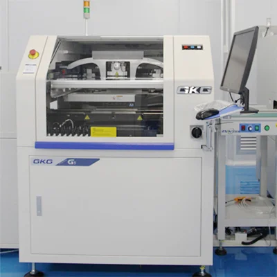
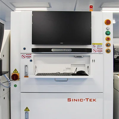
Automatic Solder Paste Printing Machine
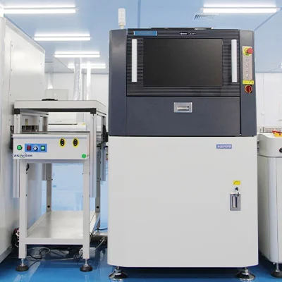
AOI Optical Inspection
Smt High-Speed Placement Machine
Nitrogen Reflow Soldering
X-Ray
Three Anti-Paint Spraying Machine
SPI Solder Paste Thickness Tester
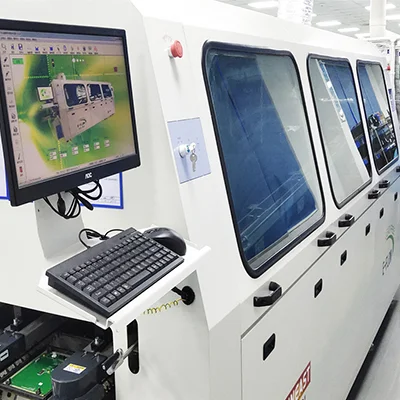
Automatic Wave Soldering Machine
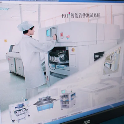
First Article Inspection

