PCB Assembly Process Video: A Step-by-Step Guide
If you’re interested in learning about the PCB assembly process, there are many videos available online that can help you understand this complex manufacturing process. These videos can be especially useful if you’re involved in the electronics industry or are considering a career in this field. By watching a PCB assembly process video, you can see firsthand how circuit boards are assembled and learn about the tools and techniques used in the manufacturing process.

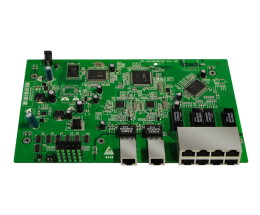
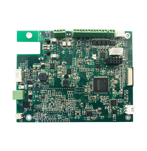
In a typical PCB assembly process video, you’ll see how the various components of a circuit board are put together to create a functional product. You’ll learn about the different types of components used in electronics, including resistors, capacitors, and integrated circuits, and see how they’re attached to the board. You’ll also see how solder is used to create electrical connections between the components and the board, and how the finished product is tested to ensure it’s working properly.
By watching a PCB assembly process video, you can gain a better understanding of how electronic devices are made and learn about the many steps involved in the manufacturing process. Whether you’re a student, hobbyist, or professional in the electronics industry, these videos can be a valuable resource for learning about the latest tools and techniques used in PCB assembly.
Overview of PCB Assembly Process

If you’re interested in learning about the PCB assembly process, there are many resources available online. One of the most informative resources is videos that show the process step-by-step. Watching a PCB assembly process video can be an excellent way to see how a PCB is created and assembled.
The PCB assembly process involves several steps, including designing the circuit board, printing the board, and assembling the components. These steps can be broken down into several sub-steps, each of which requires careful attention to detail.
One of the first steps in the PCB assembly process is designing the circuit board. This involves creating a schematic diagram of the circuit and laying out the components on the board. Once the design is complete, the board can be printed.
Printing the board involves creating a physical copy of the circuit design. This is done using a special printer that can print the circuit onto a piece of copper-clad board. Once the board is printed, it can be etched to remove the unwanted copper.
The next step in the PCB assembly process is assembling the components. This involves placing the various components onto the board and soldering them in place. This step requires careful attention to detail, as even a small mistake can cause the circuit to fail.
Overall, the PCB assembly process is a complex and intricate process that requires careful attention to detail and a high degree of skill. Watching a PCB assembly process video can be an excellent way to see how the process works and gain a better understanding of the steps involved.
Preparing for Assembly

Before starting the PCB assembly process, it’s important to prepare for it properly. This section will cover two crucial aspects of preparation: PCB design and layout, and component sourcing.
PCB Design and Layout
The PCB design and layout are critical to the success of the assembly process. A well-designed PCB will make the assembly process easier and more efficient. Here are a few things to consider when designing your PCB:
- Component placement: Place components in a logical order that will make it easier to assemble the board. Group components that are likely to be soldered together in close proximity to each other.
- Trace routing: Route traces in a way that minimizes the risk of errors during assembly. Keep traces short and straight to reduce the likelihood of solder bridges or other issues.
- Silkscreen markings: Include clear and concise silkscreen markings that will help you identify components during assembly.
Component Sourcing
Another important aspect of preparing for the assembly process is sourcing components. Here are a few tips to help you source components effectively:
- Identify your requirements: Before sourcing components, make sure you have a clear understanding of your requirements. This includes the type and quantity of components you need, as well as any specific requirements for quality or performance.
- Choose reputable suppliers: Look for suppliers with a good reputation for quality and reliability. Check reviews and ratings, and don’t be afraid to ask for references.
- Consider lead times: Make sure you factor in lead times when sourcing components. Some components may have long lead times, so it’s important to plan ahead to avoid delays.
By taking the time to properly prepare for the assembly process, you can help ensure a successful outcome.
Assembly Techniques
When it comes to PCB assembly, there are several techniques that are commonly used in the industry. In this section, we will discuss three of the most popular techniques: soldering methods, pick and place machines, and reflow soldering.
Soldering Methods
Soldering is the process of attaching components to a PCB. There are two main types of soldering methods: through-hole soldering and surface mount soldering.
Through-hole soldering involves drilling holes in the PCB and inserting the component leads through the holes. The leads are then soldered to the pads on the opposite side of the board. This method is commonly used for larger components that require more mechanical stability.
Surface mount soldering, on the other hand, involves attaching components directly to the surface of the PCB. This method is commonly used for smaller components that require a higher level of precision and speed.
Pick and Place Machines
Pick and place machines are used to automatically place components onto a PCB. These machines use a vacuum nozzle to pick up components from a feeder and place them onto the correct location on the PCB.
Pick and place machines are essential for high-volume production as they can place components at a much faster rate than manual methods. They also ensure a higher level of accuracy and consistency in component placement.
Reflow Soldering
Reflow soldering is the process of melting solder paste to attach components to a PCB. Solder paste is a mixture of tiny solder particles and flux. The paste is applied to the pads on the PCB using a stencil, and then the components are placed onto the paste.
The PCB is then heated to a high temperature in a reflow oven, causing the solder paste to melt and flow, creating a strong bond between the components and the PCB. Reflow soldering is a popular method as it is fast, efficient, and produces high-quality results.
There are several assembly techniques used in PCB manufacturing. Soldering methods, pick and place machines, and reflow soldering are just a few of the many techniques used in the industry. By understanding these techniques, you can make informed decisions about the best methods for your PCB assembly needs.
Inspection and Quality Control
After the reflow process, the PCBs must undergo a thorough inspection to ensure that they meet the required quality standards. There are three main types of PCB inspection and quality control methods: visual inspection, automated optical inspection (AOI), and functional testing.
Visual Inspection
Visual inspection is the most basic and common method of PCB inspection. It involves a visual examination of the PCB to identify any defects or issues that may affect its functionality. Visual inspection is usually carried out by trained inspectors using magnifying glasses or microscopes to identify any issues such as solder bridges, missing components, and poor solder joints.
Automated Optical Inspection (AOI)
Automated Optical Inspection (AOI) is a more advanced method of PCB inspection that uses machine vision to identify defects. AOI systems use cameras and specialized software to capture images of the PCB and analyze them for defects. AOI systems can detect defects such as missing components, incorrect component orientation, and solder defects with high accuracy and speed. Automated inspection can be done after the visual inspection to ensure that no errors are missed.
Functional Testing
Functional testing is the final stage of PCB inspection and quality control. It involves testing the PCB to ensure that it works as intended. Functional testing can be done manually or using automated test equipment. The goal of functional testing is to ensure that the PCB meets the required specifications and performs its intended functions.
In conclusion, inspection and quality control are important steps in the PCB assembly process. Visual inspection, automated optical inspection, and functional testing are the three main methods used to ensure that the PCB meets the required quality standards. By using these methods, you can ensure that your PCBs are of high quality and free of defects.


