Camera PCB Assembly: A Comprehensive Guide to Manufacturing and Quality Control
If you’re interested in learning about camera technology, you may have come across the term “camera PCB assembly.” This is the process of designing, manufacturing, and assembling printed circuit boards (PCBs) with cameras. It’s a complex task, but it’s also a critical component of many modern devices.

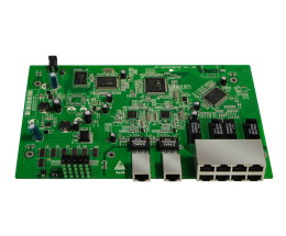
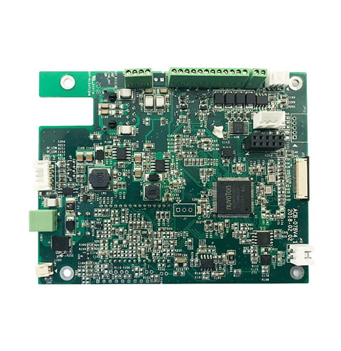
Camera PCB assembly involves creating a circuit board that supports the operation of a camera’s imaging sensor, lens assembly, image processing units, and various other components. It acts as an interface between these elements, facilitating the transfer of data, control signals, and power, while also ensuring the mechanical stability of the camera. The goal of camera PCB assembly is to produce a reliable, high-quality camera that can capture clear and detailed images.
Components of Camera PCB Assembly

When it comes to camera PCB assembly, there are several key components that are required to ensure proper functioning of the camera. These components include:
Image Sensor
The image sensor is perhaps the most important component of the camera PCB assembly. It is responsible for detecting and transferring information that is used in the development of an image. The image sensor is what allows the camera to capture the image and convert it into a digital format that can be stored or displayed on a screen. There are several types of image sensors, including CCD and CMOS sensors, each with their own advantages and disadvantages.
Lens Mount
The lens mount is the part of the camera that holds the lens in place. It is an important component of the camera PCB assembly because it determines the type of lens that can be used with the camera. There are several different types of lens mounts, including bayonet, screw, and friction mounts, each with their own unique features and advantages.
Signal Processors
Signal processors are another important component of the camera PCB assembly. They are responsible for processing the signals that are generated by the image sensor and converting them into a format that can be stored or displayed on a screen. There are several types of signal processors, including digital signal processors (DSPs) and image processors, each with their own unique features and advantages.
In summary, the image sensor, lens mount, and signal processors are the most important components of the camera PCB assembly. Each component plays a critical role in ensuring that the camera is able to capture high-quality images and process them in a way that allows them to be stored or displayed on a screen.
Design and Layout Considerations

When designing a camera PCB assembly, there are several important considerations to keep in mind. This section will cover two key aspects of the design and layout process: circuit design and PCB material selection.
Circuit Design
The circuit design is a critical component of the camera PCB assembly process. It involves the creation of a schematic diagram that outlines the electrical connections between the various components of the camera. A well-designed circuit can help ensure that the camera operates reliably and efficiently.
One important consideration when designing the circuit is to ensure that it is optimized for the specific requirements of the camera. For example, if the camera is designed for high-resolution imaging, the circuit should be designed to handle the high data rates required for this type of imaging.
Another consideration is to ensure that the circuit is designed to minimize noise and interference. This can be achieved by carefully selecting components and routing the traces in a way that minimizes crosstalk and other sources of interference.
PCB Material Selection
The choice of PCB material is another important consideration when designing a camera PCB assembly. The material used can have a significant impact on the performance and reliability of the camera.
One important consideration when selecting PCB material is to ensure that it is compatible with the specific requirements of the camera. For example, if the camera is designed for use in harsh environments, the PCB material should be able to withstand high temperatures, humidity, and other environmental factors.
Another consideration is to ensure that the PCB material is optimized for the specific requirements of the camera. For example, if the camera is designed for high-speed imaging, the PCB material should have a low dielectric constant and loss tangent to minimize signal loss and distortion.
In summary, when designing a camera PCB assembly, it is important to carefully consider the circuit design and PCB material selection. By taking these factors into account, you can help ensure that the camera operates reliably and efficiently, and meets the specific requirements of your application.
Assembly Process
When it comes to the assembly process of camera PCBs, there are two main techniques: soldering and automated assembly. Both techniques require precision and expertise to ensure that the camera PCB functions correctly.
Soldering Techniques
Soldering is a traditional technique used to attach electronic components to PCBs. In camera PCB assembly, soldering is used to attach the camera components to the PCB. This process involves melting a metal alloy, known as solder, to create a connection between the camera component and the PCB.
There are two main types of soldering techniques used in camera PCB assembly: through-hole soldering and surface mount technology (SMT). Through-hole soldering involves drilling holes in the PCB and inserting the camera components through the holes. The components are then soldered in place on the other side of the PCB. SMT, on the other hand, involves attaching the camera components directly to the surface of the PCB.
Automated Assembly
Automated assembly is a newer technique used in camera PCB assembly. This technique involves using machines to place the camera components onto the PCB. Automated assembly is faster and more precise than soldering, making it the preferred technique for high-volume production.
Automated assembly machines use a variety of techniques to place the camera components onto the PCB. Some machines use pick-and-place technology, where a robotic arm picks up the camera component and places it onto the PCB. Other machines use jetting technology, where a jet of glue is used to attach the camera component to the PCB.
Both soldering and automated assembly techniques are used in camera PCB assembly. Soldering is a traditional technique that is still used today, while automated assembly is a newer technique that is faster and more precise. Regardless of the technique used, camera PCB assembly requires precision and expertise to ensure that the camera functions correctly.
Testing and Quality Control
When it comes to camera PCB assembly, testing and quality control are crucial steps to ensure that the final product meets the required specifications. In this section, we will discuss two types of testing that are commonly used in camera PCB assembly: functional testing and reliability testing.
Functional Testing
Functional testing is a type of testing that verifies whether the camera PCB functions as intended. This test is usually performed after the PCB has been assembled and before it is shipped to the customer. The purpose of functional testing is to ensure that the camera PCB operates correctly and meets all the required specifications.
During functional testing, the camera PCB is connected to a test system that simulates the camera’s operation. The test system checks the camera PCB’s functionality by performing various tests, such as checking the camera’s image quality, color accuracy, and resolution. If the camera PCB fails any of these tests, it is sent back for rework.
Reliability Testing
Reliability testing is a type of testing that verifies whether the camera PCB can perform consistently over a long period of time. This test is usually performed after the functional testing and before the camera PCB is shipped to the customer. The purpose of reliability testing is to ensure that the camera PCB can withstand the stresses of real-world use and operate reliably over its expected lifespan.
During reliability testing, the camera PCB is subjected to various environmental conditions, such as temperature and humidity, to simulate real-world use. The camera PCB is also subjected to various stress tests, such as thermal cycling and vibration testing, to ensure that it can withstand the stresses of real-world use. If the camera PCB fails any of these tests, it is sent back for rework.
Testing and quality control are essential steps in camera PCB assembly. Functional testing ensures that the camera PCB operates correctly and meets all the required specifications, while reliability testing ensures that the camera PCB can perform consistently over a long period of time. By performing these tests, manufacturers can ensure that their camera PCBs are of high quality and meet the needs of their customers.
Emerging Technologies in Camera PCBs
If you are interested in camera PCB assembly, you should know about the emerging technologies that are changing the industry. Two of the most exciting developments in camera PCBs are 3D integration and flexible PCBs.
3D Integration
3D integration is a technology that allows multiple layers of PCBs to be stacked on top of each other. This technology is particularly useful for camera PCB assembly because it allows for more compact designs and better signal integrity. With 3D integration, manufacturers can create camera PCBs that are smaller, lighter, and more powerful than ever before.
Flexible PCBs
Flexible PCBs are another emerging technology that is changing the camera PCB assembly industry. As the name suggests, flexible PCBs are designed to be flexible, which allows them to be bent, twisted, and folded into a variety of shapes. This technology is particularly useful for camera PCBs because it allows manufacturers to create cameras with unique form factors.
Flexible PCBs are also more durable than traditional PCBs because they are less likely to crack or break under stress. This means that cameras with flexible PCBs are better able to withstand drops, impacts, and other types of damage.
In addition to 3D integration and flexible PCBs, there are many other emerging technologies that are changing the camera PCB assembly industry. By staying up-to-date with these developments, you can ensure that your camera PCBs are always on the cutting edge of technology.


